1. Intro
The circuit is in fact the topology according to the Douglas Self's Blameless Amplifier discussed in his book Audio Power Amplifier Design Handbook and also on his website
http://www.douglas-self.com/ampins/dipa/dipa.htm
http://www.douglas-self.com/ampins/dipa/dpafig33.gif
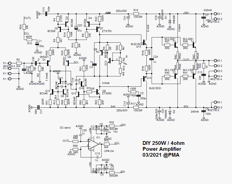
This is the complete schematics of the amplifier that I built
It was built into my prototype case with two 300VA toroidal transformers, that are needed for the dual-mono, which determined the size of the PCB and also components placement and drilling. The case is 19" 4U, dimensions 450 x 415 x 180 mm. It has big side heatsinks and can accommodate 2x250W amplifier concept with long-term full-power capacity.
This is the amplifier built in the prototype 19" 4U case


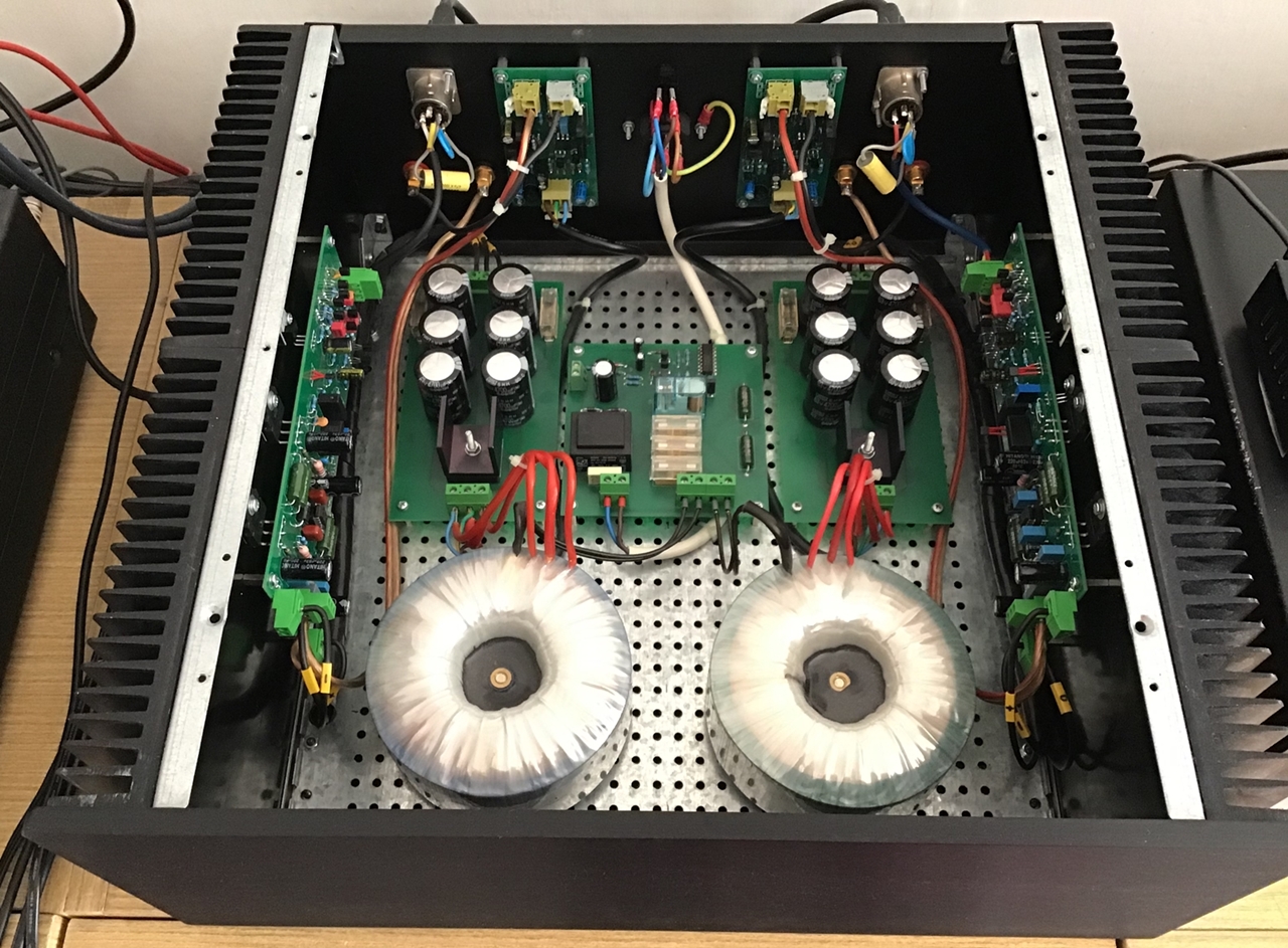
The design is dual mono. There are two transformers, two rectifier-filter boards, two amplifier boards and two delayed start/DC protection boards inside the case. Two MJL3281/1302 output pairs make 250W/4ohm power possible with respect to SOA (Safe Operating Area) of the transistors. It is possible to use speaker complex load that does not fall below 4 ohm in its impedance/frequency plot. The amp may drive purely resistive load of 2 ohm up to full output swing and still stay inside allowed SOA boundaries. The amp is able to drive capacitive load up to 4ohm//2.2uF remaining stable.
2. Functional sample parameters
3. Measurements (according to IEC 60268-3)
3.1. Input characteristics
3.1.1. Rated source impedance - 100 ohm
3.1.2. Input impedance - 66kohm/20Hz, 65kohm/1kHz, 30kohm/10kHz, 17kohm/20kHz
3.2. Output characteristics
3.2.1. Rated load impedance - 4ohm (or more)
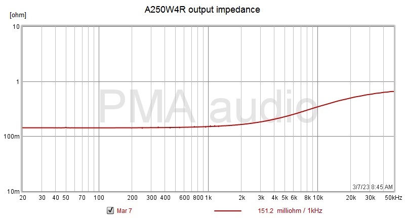
3.2.2. Output source impedance (including SSR protection board) - 0.15 ohm at 1kHz, 0.35 ohm at 10kHz
3.2.3. Output power (distortion limited at 1%) - 2 x 280W/4ohm
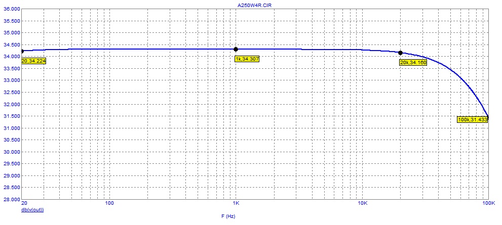
3.2.4. Gain under standard measuring conditions - 34.3 dB
3.3. Overload
restoring time
3.3.1. Characteristic to be specified
The time interval (which occurs after the amplifier working under
standard measuring conditions is overloaded by a certain amount
for a specified period) between the moment when the input voltage
is restored to its original value and the moment when the output
voltage has again reached its original value within specified
limits
3.3.2. Method of measurement
a) The amplifier is brought under standard measuring conditions.
b) The source e.m.f. is increased by 20 dB during a time interval
of less than one-quarter
period of the input signal and kept at this value for
approximately 1 s.
c) The source e.m.f. is then reduced to its initial value during
a time interval of less than onequarter
period of the input signal.
d) The time that passes before both the positive and the negative
output peak voltages have
reached their final value, within 1 dB unless otherwise specified,
is measured by means of
a suitable calibrated oscilloscope.
3.3.3. Measurements of overload restoring time
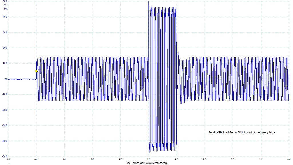
Full record. Rated power is 250W/4ohm => standard measuring power is 25W/4ohm (10Vrms). 20Hz frequency.
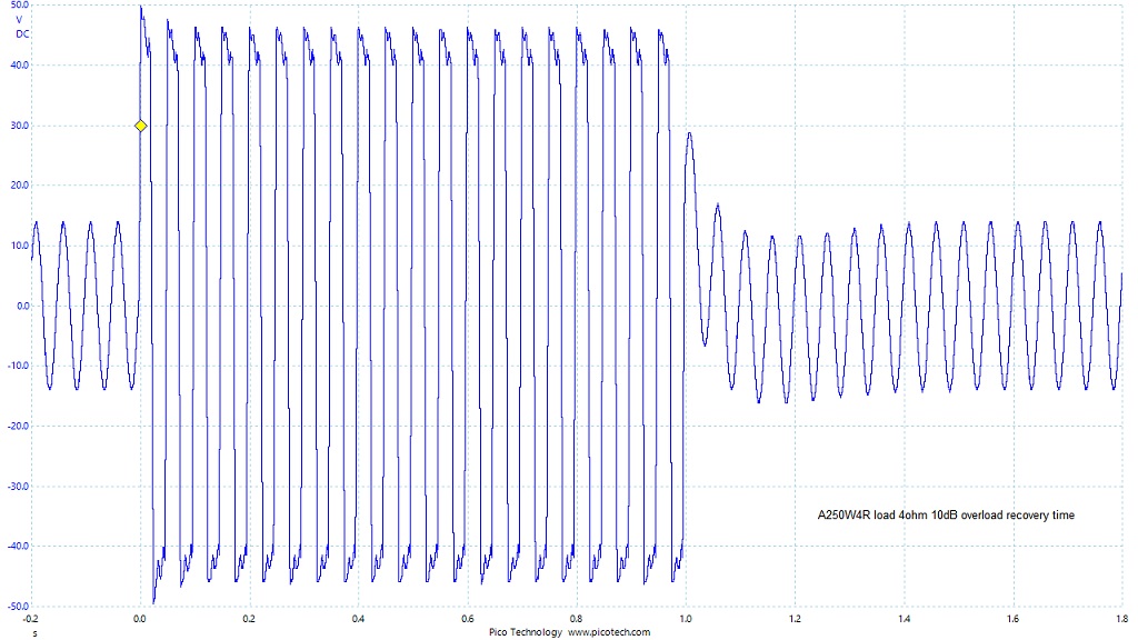
Transition area zoomed. Please note power supply ripple superposition on the clipped dignal.
The same measurements at 1kHz
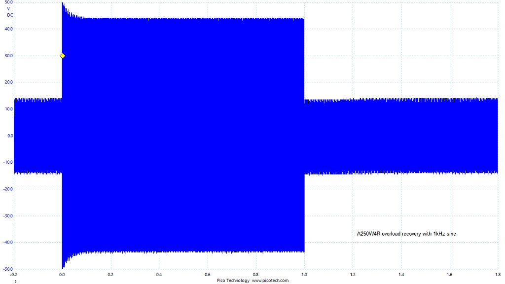
Full record.
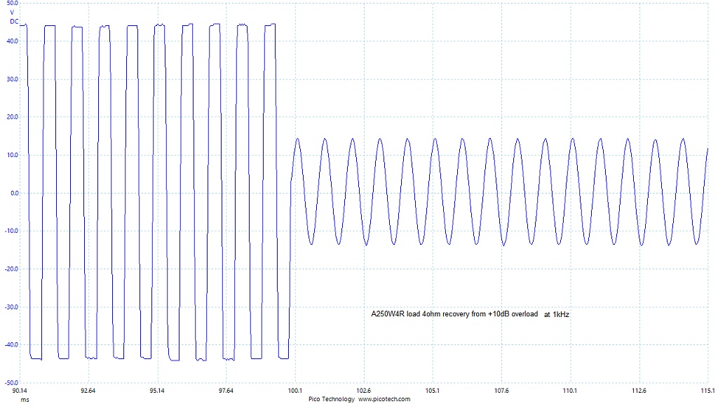
Transition area zoomed.
Please keep in mind that overload in this test is +10dB.
3.4. Responses
3.4.1. Gain-frequency response
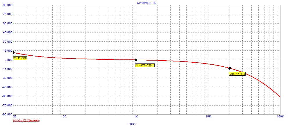
3.4.2. Phase-frequency response
3.5. Amplitude non-linearity
3.5.1. Rated total harmonic distortion - 0.1%
3.5.2. Total harmonic distortion under standard measuring conditions - 0.01%
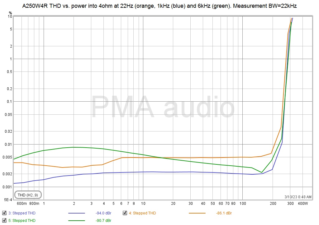
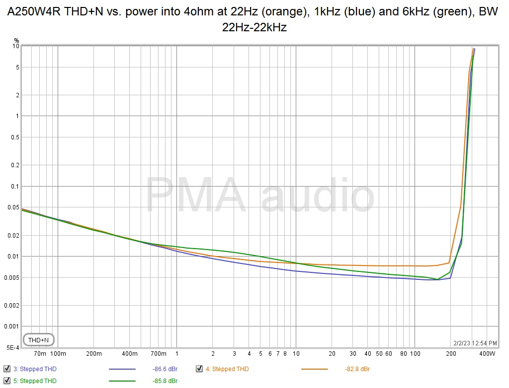
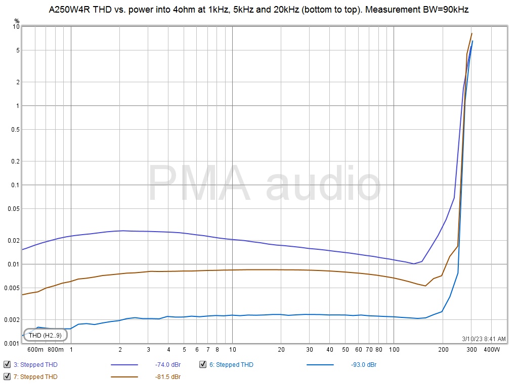
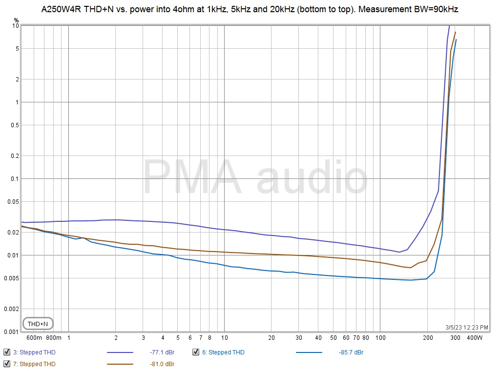
3.5.3. Total harmonic distortion as a function of amplitude and frequency
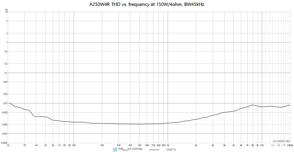
3.5.4. Distortion vs. frequency - 150W/4ohm/BW45kHz
4. Testing this amplifier in the bridged mode
A250W is a dual-mono
amplifier, two completely separated power amplifiers with
separate power supplies, all in one 4U x 19” case. The
inputs are only unbalanced RCA. To make a bridged amplifier, it
is necessary to tight output “Lo” speaker terminals of
both channels together and the load is there connected between
“Hi” speaker terminals of the left and right channels.
This will interconnect power signal grounds of both channels. Now,
we must not connect the signal grounds of the left and the right
RCA input connectors together, as it would create a ground loop
including the high current speaker ground returns and thus
destroy the S/N of the amplifier, resulting in hum and buzz. At
the same time, we must invert signal for one of the inputs to get
the doubled voltage swing between the “Hi” output
terminals of the left and right channel. This is the trick of the
bridged amplifier, we get twice of output voltage of the single
amplifier channel, thus four time the power (in theory). But, now
any of the two channels sees half of the load impedance and must
deliver the two times more current. So, the output transistors
are much more stressed.
My test setup looks as follows:
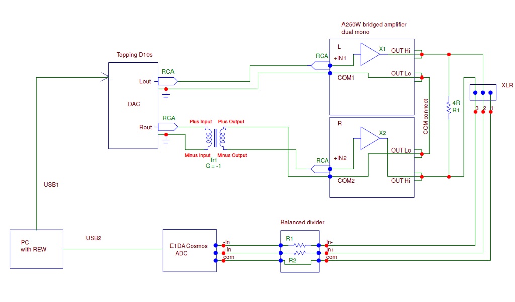
L and R channels of the dual
mono amplifier are completely separated. They are then connected
by the “COM connect” wire between the OUT Lo terminals
of both channels. The load is connected between OUT Hi terminals.
RCA input of the left channel is driven directly, input of the
right channel is driven via the 1:1 link transformer in opposite
polarity, which assures inverted polarity at the OUT Hi of the
right channel. Load is thus not tied to signal ground and the
measurement must be differential, as shown in the schematics.
Measurements in bridged mode
I have measured THD vs. output level for 4ohm, 6.8ohm and 8ohm
resistive load. Then I have also measured a burst power into 4ohm.
Below is the comparison of THD+N vs. power at 1kHy into 4 ohm and
8 ohm load in the normal single chanel mode and bridged mode:

Burst power was alsomeasured, by 7 periods of 100Hz sine, total duration 70ms, rectangular window (no smoothing of signal rise and decay). Burst power measured is 770W/4ohm.
page created 03/2021, last edited : February 4, 2025