Distortion analysis of basic JFET circuits
This page has been initiated by John Curl in Blowtorch thread at www.diyaudio.com.
We have started to analyze distortion spectra of single JFET and differential JFET pair both for ideal and real devices. Our goal is to continue with more sophisticated structures like complementary differential pair and differential pair with folded cascode.
Let me repeat the results for single JFET and differential JFET pair at first
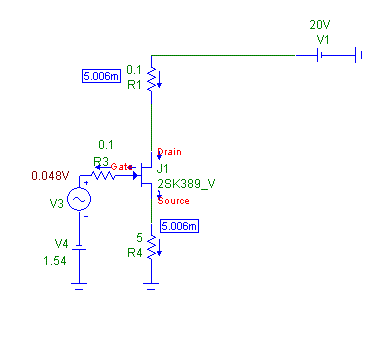
1. Single JFET
1.1. Single JFET, zero lambda
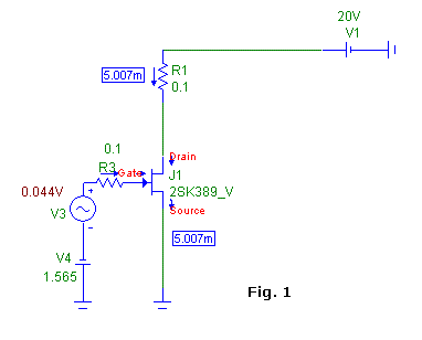
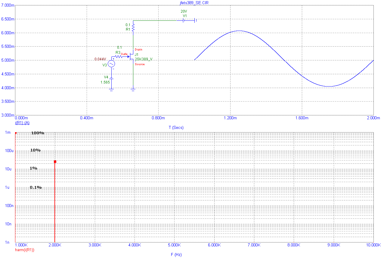
For single JFET, the analyzed circuit is as follows:
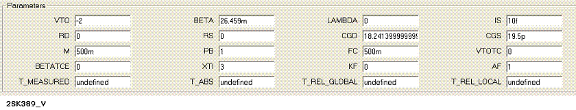
The device used is 2SK389_V. The spice model of this device has lambda = 0, i.e. the transfer function meets square law. The model is as follows:
 (model 1)
Distortion spectrum of this circuit with the model shown is shown in Link 1 .This is a distortion of JFET drain current for constant Vds. It contains only pure 2nd harmonic component, with value of some 2.5% for given model, operating current, and input voltage.
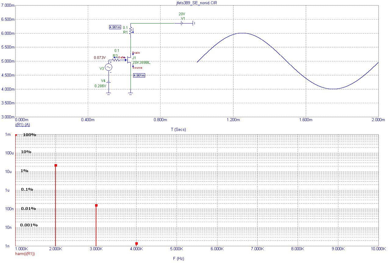
1.2. Single JFET, non-ideal device
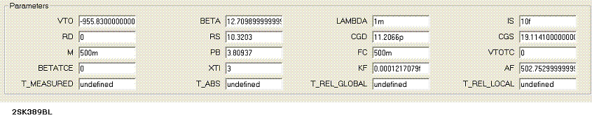
For the same circuit (Fig. 1) we use a model of non-ideal device. This model has non-zero lambda (channel-length modulation) :
 (model 2)
Now distortion spectrum is shown in Link 2 . We can see that 3rd and 4rd harmonic component appeared, as a result of non-zero channel-length modulation. The reason of appearance of new harmonic components can be derived from JFET transfer function:
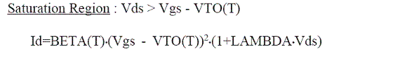 (equation 1)
where the effect of lambda can be seen.
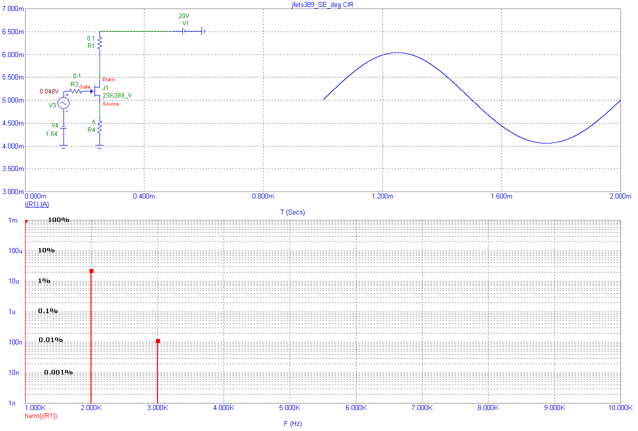
1.3. Single JFET, zero lambda, emitter degeneration
Now we analyze single device with zero lambda (meets square law transfer function), but with emitter (source) resistor added.
For this circuit, distortion is in Link 3 . 3rd harmonic has appeared, as a result of voltage drop on R4 effect on Id (equation 1).
1.4. Single JFET, zero lambda, no degeneration, drain resistor
In case we increase value of R1 to become a drain load, for the reason of voltage output, again we create higher harmonics than 2nd. The reason is again seen in equation 1, Vds is not constant, the (1 + lambda.Vds) becomes non-zero, and Id does not follow pure square law.
2. JFET differential pair
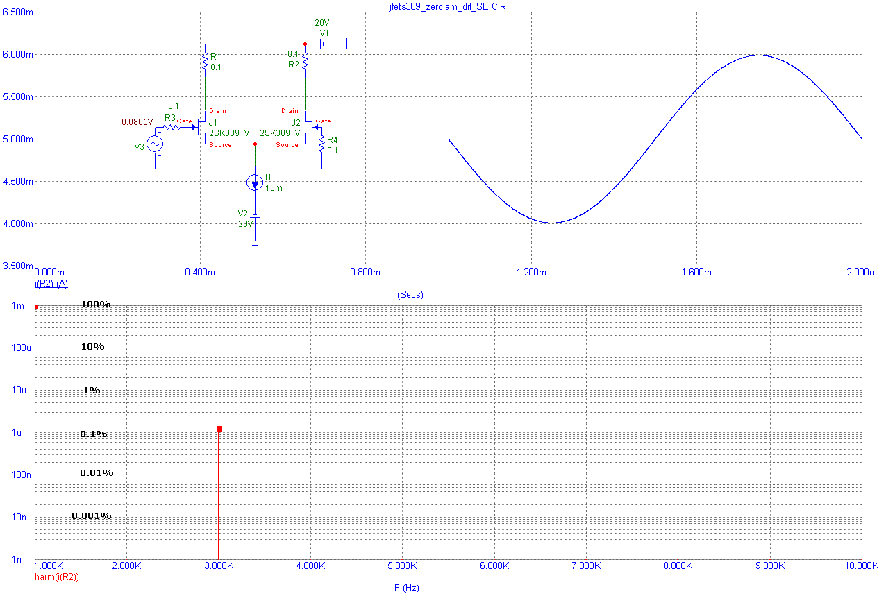
2.1. JFET differential pair, lambda=0, single-ended input, single-ended output
We start our JFET differential pair analysis with single-ended input and single-ended output, very usual praxis in audio amplifiers.
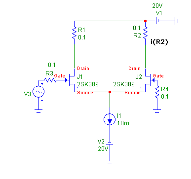
The input signal is voltage V3, output is current i(R2), with R2 value negligible. Distortion of such circuit is shown in Link 4 . It is pure 3rd harmonic of some 0.1% for given conditions.
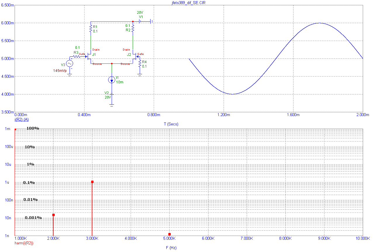
2.2. JFET differential pair, non-zero lambda
For same conditions as in article 2.1., only JFET model has non-zero lambda (model 2), we can see distortion in Link 5 . Now, 2nd harmonic has appeared and also very small 5th.
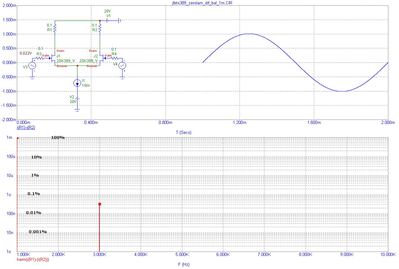
2.3. JFET differential pair, balanced input, balanced output
Now we have JFET differential pair with true differential input and true differential output. It sees voltage difference at the input and current difference at the output.
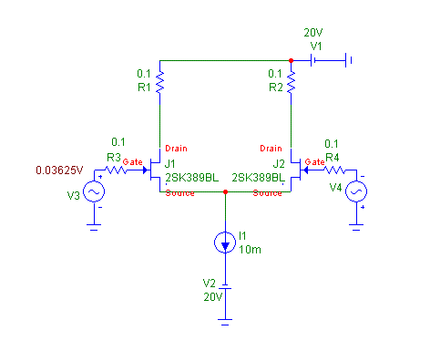
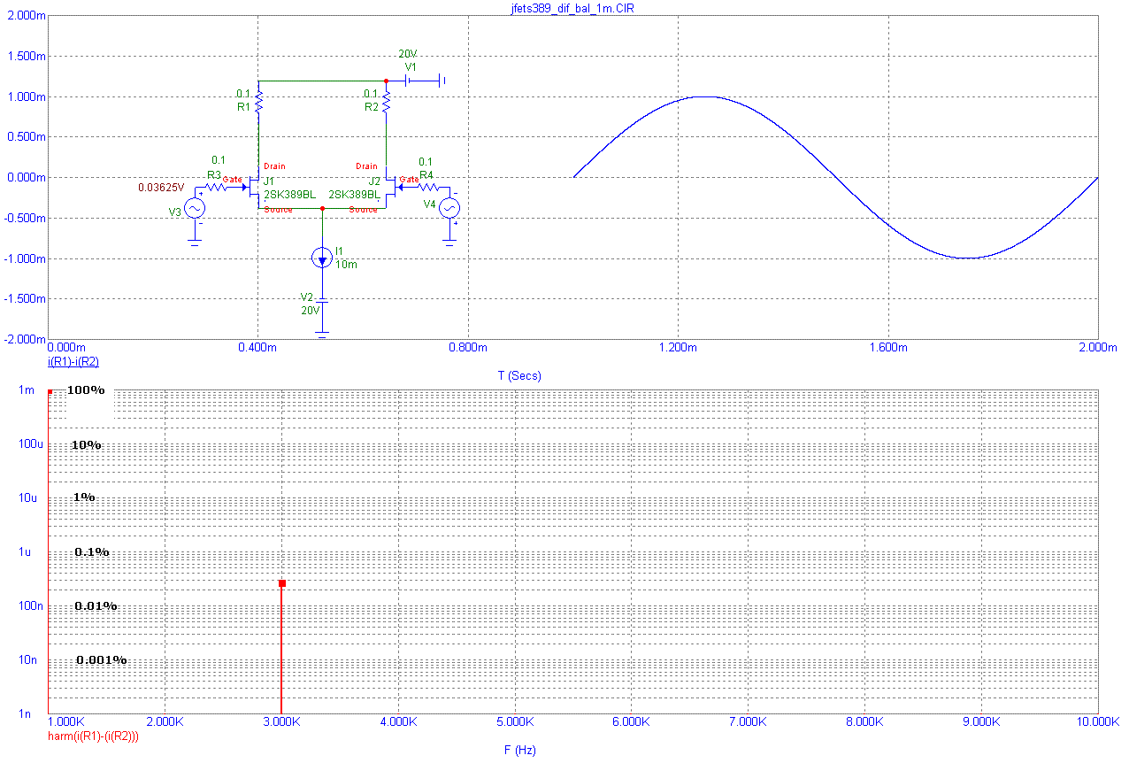
First we assume devices with lambda=0. Distortion spectrum is in Link 6 . It is pure 3rd harmonic, 0.03%. Now we take non-ideal device with lambda = 1m (model 2), distortion is in Link 7 . It is again only pure 3rd harmonic. That means, for true differential pair, even with nonideal devices, no even harmonics were created. The condition is symmetry of input, balanced output and same devices.
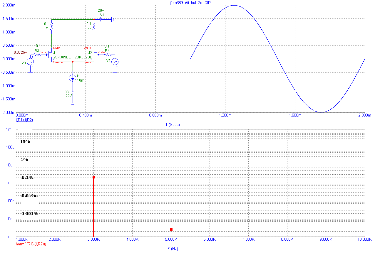
We increase output current now to 2mA, everything else same. Distortion is in Link 8 . Distortion is odd harmonics only, but we can see very small 5th, 0.00025%, has appeared.
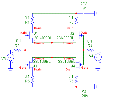
3. Complementary differential pair
3.1. Complementary differential pair, fully balanced, current output
is our next step:
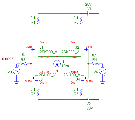
Distortion of this circuit is in Link 9 . Distortion is pure 3rd, and decreased to 0.006%, for 1mA output current.
In case we replace the I1 constant current source by short, as recommended by John Curl, we get substantial reduction of distortion to absolutely negligible value, see Link 10 .
However, we need some means to control drain current, as it depends on Vto of JFEts, and with short it may become too high. Or we use another device grade, for BL we get Id = 10mA approx, like here in the Link 10.
4. Gain control for complementary differential pair
To control the gain, we introduce a resistor between left and right halves of the circuit.
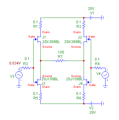
The R7 resistor creates local feedback, the higher the resistor value, the lower gain. Let's see effect of resistor value to distortion spectrum.
4.1. R7 = 10R
Distortion spectrum for R7 = 10R is shown in Link 11. It is pure 3rd harmonic of 0.0007%, nothing else is seen till -180dB.
4.2. R7 = 100R
Distortion spectrum for R7 = 100R is shown in Link 12. The 3rd is reduced to 0.0002%, but we can see higher harmonics start to appear, though very low in magnitude.
So this kind of local feedback reduces overall distortion, but creates new harmonic components again.
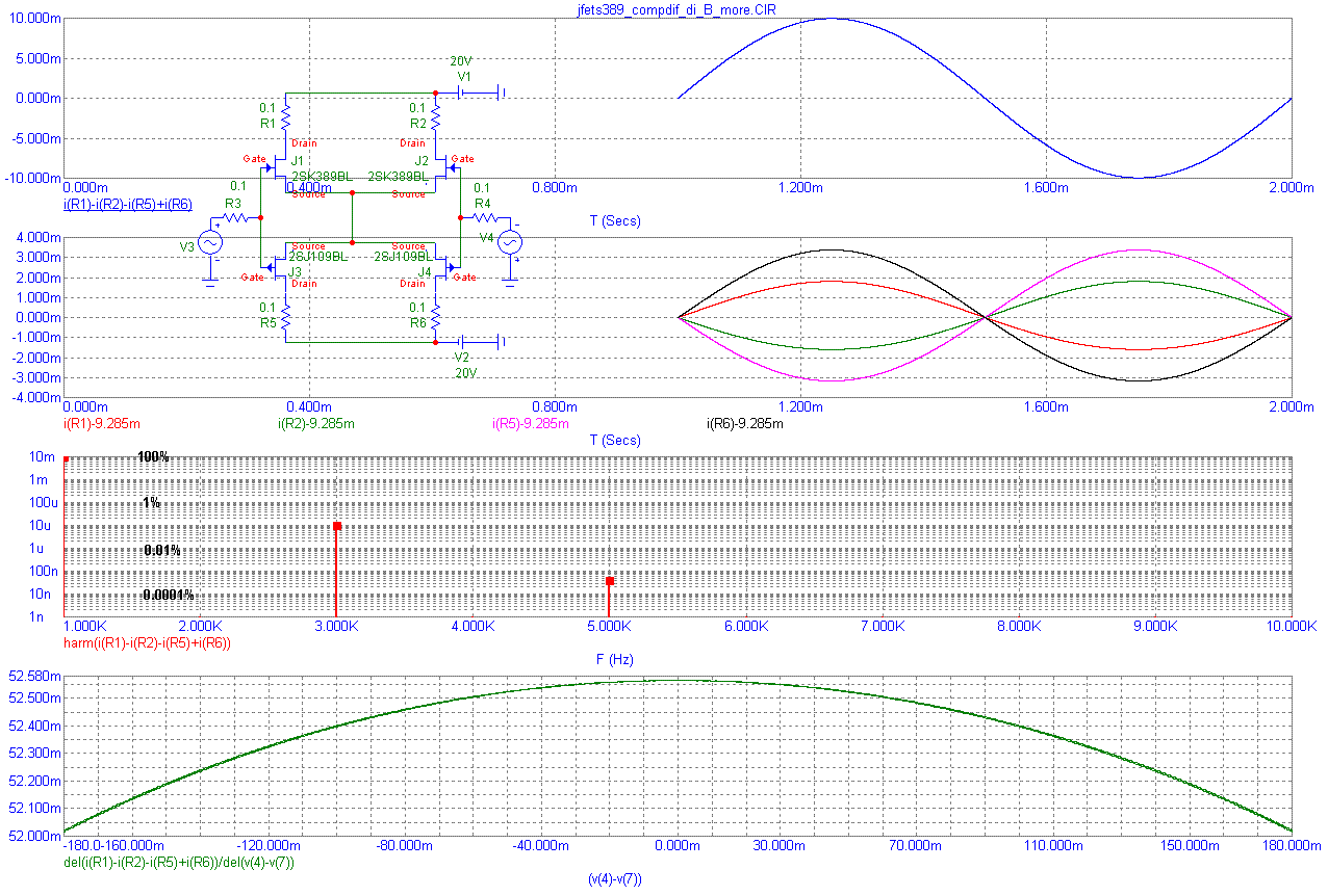
5. Influence of matching of N and P halves in complementary differential pair
Let us return to complementary differential pair with N and P halves directly connected.
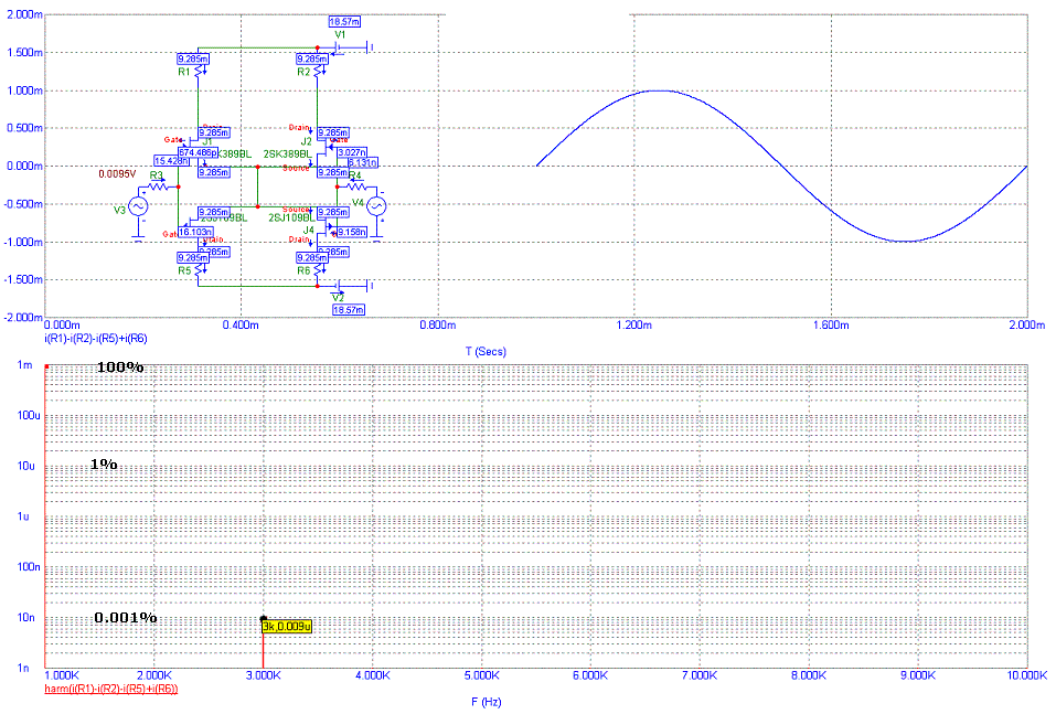
In case of 2SK389BL/2SJ109BL model devices, Id = 9.285mA. We shall now investigate distortion for output current 10mA, see Link 13. Distortion rised and we can see also 5th harmonic has appeared. We also monitor all 4 drain currents. As we can see, they are not equal, but N a P halves differ. The reason is different threshold voltage and transconductance of N and P jfets, see model parameters:
*** N Channel JFET
.MODEL 2SK389BL NJF (VTO=-955.83m BETA=12.7099m LAMBDA=1m RS=10.3203
+ CGD=11.2066p CGS=19.1141p PB=3.80937 KF=1.217079E-019 AF=502.753m)
*** P Channel JFET
.MODEL 2SJ109BL PJF (VTO=-418.894m BETA=83.8035m LAMBDA=1m RS=11.0887
+ CGD=71.6975p CGS=61.6464p PB=1.85382 KF=7.879067E-018 AF=499.474m)
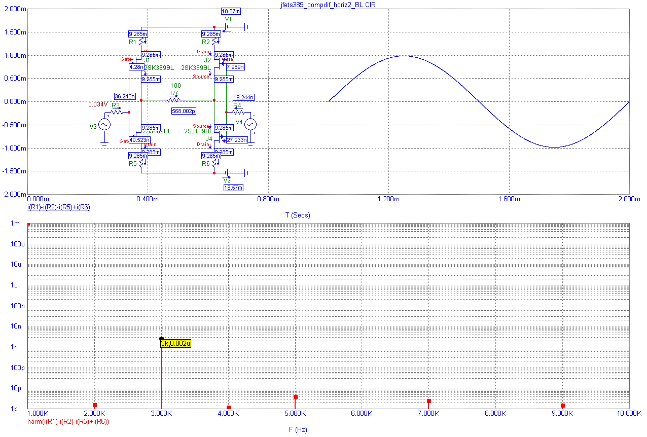
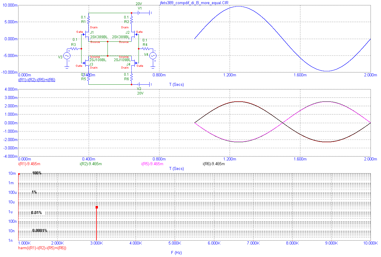
We shall try to make the models more similar by keeping VTO=-955.83m and BETA=12.7099m for both N and P jfet. Now let us try distortion again, see Link 14. The 5th harmonic disappeared, 3rd is reduced and all 4 drain currents are same. So, to keep the lowest distortion and avoid higher harmonics, we need to have N and P jfets as equal as possible.
to be continued ....
Pavel Macura, 04/2008